Our latest blog is from Dr Robert Hoye, a Lecturer in the Department of Materials at Imperial College London, who recently gave a webinar in our Sustinable Power series. In this blog, Dr. Hoye discusses the potential of semiconducting compounds based on the element bismuth for safely and sustainably harvesting energy from the sun and indoor light sources to power electronics.
The need for sustainable solar cells
The UK has committed itself to achieving net-zero CO2 emissions by 2050, and other countries are following suit. One of the critical pillars to achieving this goal will be to decarbonise the power generation sector. Photovoltaics, or solar cells, convert sunlight to electricity without emitting any CO2, and are a critical source of renewable energy. But photovoltaics are not only needed on rooftops or in solar farms to harvest solar energy, they are also needed to harvest indoor lighting to power an exponentially increasing number of small, autonomous devices used to create the smart homes and workplaces of the future. Currently, the industry-standard material used in photovoltaics is silicon – either crystalline silicon for solar energy harvesting, or amorphous silicon for harvesting indoor light. The best crystalline silicon solar cells have now approached their limits in efficiency, whereas amorphous silicon is less than 10% efficient under indoor lighting. Identifying routes to increase efficiencies and lower the ratio of cost to power produced will be important for accelerating the deployment of photovoltaics.
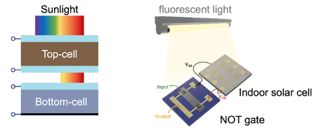
Over the past decade, the photovoltaics community has discovered a new class of lead-halide perovskites. These materials hold promise for enabling practical routes to increase efficiencies. Lead-halide perovskites absorb visible light, which is complementary to crystalline silicon (which absorbs near-infrared light). Perovskite solar cells can therefore be used in tandem with silicon to exceed the efficiency limit of silicon single-junction devices (see Figure 1). Moreover, efficient perovskite solar cells can be made using simple, low-temperature fabrication processes. Combining perovskites with silicon in tandem devices can therefore allow increases in efficiency without substantially increasing cost, offering the prospect of reducing the cost to power ratio of solar cells. Furthermore, perovskites have already been shown to be nearly four times as efficient as amorphous silicon in harvesting indoor light.
But a critical challenge is the toxicity of lead in perovskites, which is present in an easily-accessible soluble form. Although researchers are developing methods to sequester lead or safely recycle perovskite solar cells, it is important to identify safer alternatives that can replicate the ability of lead-halide perovskites to be efficient despite having many defects when made by low-cost methods. This property is called defect tolerance.
Bismuth – the green element in poisoner’s corridor
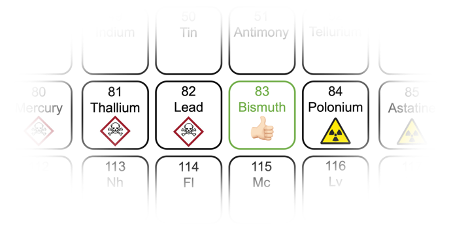
Over the past five years, the spotlight has been on compounds based on bismuth. Bismuth is an element located in the ‘poisoner’s corridor’ of the periodic table (Figure 2). It sits next to lead, thallium and mercury on one side, and radioactive polonium and astatine on the other. Surprisingly, bismuth-based compounds have demonstrated very little evidence of toxicity. Bismuth subsalicylate, for example, is the active ingredient in over-the-counter stomach medicine ‘Pepto-Bismol’.
Nevertheless, bismuth has many electronic properties that are similar to its toxic neighbours. These include a large electron cloud, strong mixing of electronic orbitals, and the formation of a stable ionised state that has the same configuration of electrons as lead ions. Moreover, bismuth is available in sufficient quantities to be considered for commercial use. The US Geological Survey estimates global reserves of bismuth to be 370,000 tonnes, which is an order of magnitude larger than tellurium, which is already commercially used in solar cells.
Promising defect tolerance and stability in air
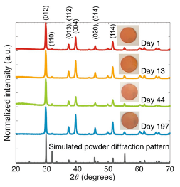
One of the many bismuth-based compounds explored is bismuth oxyiodide. This is a red, layered compound that absorbs visible light. We and co-workers showed through experiments and calculations that this material tolerates defects in a similar way to lead-halide perovskites. Bismuth oxyiodide thin films are grown using a vapour-based method that can be scaled-up to the industrial level. Furthermore, we showed that bismuth oxyiodide thin films are stable in ambient air, with no degradation over the 197 day testing period (Figure 3). This is substantially improved over methylammonium lead iodide perovskite, which degrades within 5 days under the same conditions. These results are published in Advanced Materials.
Bismuth-based semiconductors in solar cell devices
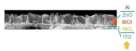
We made a fully-inorganic device structure for bismuth oxyiodide solar cells (Figure 4). These devices demonstrated an external quantum efficiency of up to 80% at 450 nm wavelength. This means that at blue wavelengths, 80% of photons were converted to electrons, which shows that photogenerated charge-carriers can be efficiently extracted in this material under short-circuit conditions. However, the power conversion efficiencies are currently low, at approximately 2%. This is partly because the material absorbs visible light but not near-infrared light (which is a large part of the solar spectrum), thus limiting the total photocurrent generated.
But we recently showed bismuth oxyiodide to be more efficient in harvesting indoor light, which is distributed only over the visible wavelength range. Bismuth oxyiodide solar cells reached 4.4% efficiency under fluorescent lighting, which is within the range of efficiencies reported for commercialised indoor photovoltaics. We showed that the current bismuth oxyiodide solar cells are sufficient for powering NOT gates, an important building block for logic circuits (Figure 1, right). To determine the ultimate potential of bismuth oxyiodide, we calculated the maximum efficiency if all light absorbed became photocurrent, and found that these efficiencies reached over 40%. These results are published in Advanced Energy Materials.
What next?
The performance of bismuth oxyiodide could be improved by tailoring the charge transport layers and improving the morphology of the films. More broadly, other bismuth-based solar cells also face similar challenges of absorbing visible light rather than near-infrared light. Until now, these materials have only been considered for outdoor photovoltaics, but we predict that these materials have more promise for indoor light harvesting, with maximum efficiencies for fully optimised devices potentially reaching the 40–60% range.
Another broader challenge is that the design rules for pinpointing bismuth-based materials that could replicate the defect tolerance of the perovskites are incomplete. So far, only a handful of the bismuth-based compounds identified have been shown to be defect tolerant. The challenges of pushing forward the inverse design of such materials, and the potential to incorporate machine learning approaches to accelerate their discovery is discussed in our upcoming review (pre-print available following this link). This review is highlighted in Nature Physics.
Finally, although the field is razor-focussed on the discovery of bismuth-based materials for photovoltaics, it is important to also appreciate that these compounds may hold greater promise for alternative applications. For example, bismuth is a heavy element, meaning that bismuth-based compounds can effectively absorb ionising radiation (such as X-rays). These materials can make cheaper, non-toxic radiation detectors that can detect lower and safer dose levels than the current commercial technology. Other applications include white light phosphors, memory storage devices or photocatalysts for producing clean fuels from sunlight.
Biography:
Dr Robert Hoye is a Lecturer and Royal Academy of Engineering Research Fellow in the Department of Materials at Imperial College London. He leads the Energy Materials & Devices Group, which focuses on the development of thin film semiconductors for clean energy conversion. Dr. Hoye completed his PhD at the University of Cambridge (2012-2014), before being a Postdoctoral Research Associate at MIT (2015-2016). In 2016-2019, he returned to the University of Cambridge as a College Research Fellow. From 2018, he took-up the Royal Academy of Engineering Research Fellowship, initially at Cambridge, before moving to Imperial College as a Lecturer in January 2020.

[…] for applying the material in a broad range of alternative applications. One such application is for indoor light harvesting. These energy-havesting devices are needed to power low-cost, low-power electronic devices that can […]
LikeLike